Showing posts with label detector. Show all posts
Showing posts with label detector. Show all posts
Friday, September 27, 2013
Simple Audio Peak Detector
This audio peak detector allows a pair of stereo channels to be monitored on a single LED. Identical circuitry is used in the left and right channels. Use is made of the switching levels of Schmitt trigger NAND gates inside the familiar 4093 IC. The threshold level for gate IC1.A (IC1.B) is set with the aid of preset P1, which supplies a high impedance bias level via R2 (R1). When, owing to the instantaneous level of the audio signal superimposed on the bias voltage by C3 (C2), the dc level at pins 1 and 2 (5 and 6) of the Schmitt trigger gate drops below a certain level, the output of IC1.A (IC1.B) will go High.

This level is copied to the input of IC1.C via D2 (D1) and due to the inverting action of IC1.C, LED D3 will light. Network R3-C1 provides some delay to enable very short audio peaks to be reliably indicated. Initially turn the wiper of P1 to the +12 V extreme — LED D3 should remain out. Then apply ‘line’ level audio to K1 and K3, preferably music with lots of peaks (for example, drum ‘n bass). Carefully adjust P1 until the peaks in the music are indicated by D3. The circuit has double RCA connectors for the left and right channels to obviate the use of those rare and expensive audio splitter (‘Y’) cables.
Continue Read...

This level is copied to the input of IC1.C via D2 (D1) and due to the inverting action of IC1.C, LED D3 will light. Network R3-C1 provides some delay to enable very short audio peaks to be reliably indicated. Initially turn the wiper of P1 to the +12 V extreme — LED D3 should remain out. Then apply ‘line’ level audio to K1 and K3, preferably music with lots of peaks (for example, drum ‘n bass). Carefully adjust P1 until the peaks in the music are indicated by D3. The circuit has double RCA connectors for the left and right channels to obviate the use of those rare and expensive audio splitter (‘Y’) cables.

Monday, September 2, 2013
SD2 Smoke Detector
This smoke detector circuit diagram is based on the SD2 CMOS Photo-Electric Smoke Detector Integrated Circuit manufactured by Supertex INC and include almost all needed components to build a very simple and high efficiency smoke detector project .As you can see , this smoke detector circuit diagram is very simple an require few external components .
SD2 Smoke Detector Circuit diagram

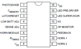
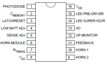 The LED predriver output pulses an external transistor which in turn, switches on the infrared light emitting diode at a very low duty cycle. The desired IR LED pulse period is determined by the value of the externai timing resistor. The Smoke Sensitivity is adjustable through a trimmer resistor which varies the IR LED puise width. The light sensing element is a silicon photovoltaic cell which is held at near zero bias to minimize leakage currents. The circuit can detect signals as low as 1 mV and generate an alarm. The IR LED pulse repetition rate increases when smoke is detected. The IR diode can be RCA Type SG 1010A or Spectronics Type SE 5455-4 Clairex and the IR Photo detector can be Vactec VTS4085 .
Because the SD2 CMOS Photo-Electric Smoke Detector IC is designed for use in low power, battery operated, consumer applications it needs a 9 volts DC power supply (or a 9 volts battery ).
SD2 Smoke Detector Circuit diagram

Because the SD2 CMOS Photo-Electric Smoke Detector IC is designed for use in low power, battery operated, consumer applications it needs a 9 volts DC power supply (or a 9 volts battery ).
Sunday, September 1, 2013
Metal Detector Based on the TDA0161
These metal detector circuit diagram is based on the TDA0161 monolithic integrated circuit , designed for metallic body detection by detecting the variations in high frequency Eddy current losses. For detecting metals , TDA0161 require an external LC tuned circuit .
Metal Detector Circuit diagram

Output signal is determined by supply current changes. Independent of supply voltage, this current is high or low according to the presence or the absence of a close metallic object. This metal detector circuit use two LEDs , which offer an visual indication of presence or absence at a metals ,around the coil . To adjust the circuit you need to make sure there is no metal near the coil and then set the fine adjustment to a "Mid position". After that you need to adjust the course adjustment to turn on the LED and , adjust the fine adjustment to turn off the LED.
This detector electronic circuit operates over a wide range input voltage of 4 -35 volts . If you want you can use other values for the Cx capacitor and for L1 inductor ( changing this value will affect the frequency oscillation and the detection range ) .
Metal Detector Circuit diagram

This detector electronic circuit operates over a wide range input voltage of 4 -35 volts . If you want you can use other values for the Cx capacitor and for L1 inductor ( changing this value will affect the frequency oscillation and the detection range ) .
Thursday, August 8, 2013
Spike Detector For Oscilloscopes
Dynamic flip-flops ignore pulses at their inputs that are shorter than 40 ns or do not have TTL levels. This means that TTL flip-flops are poorly suited to capturing noise pulses having unknown durations and magnitudes. Anyone who has ever tried to observe very short laser pulses (15–25 ns) is familiar with this problem. By contrast, this circuit can detect impulses with widths less than 8 ns and amplitudes between +100 mV and +5 V. The heart of this circuit is formed by a MAX903, a very fast comparator with internal memory. The IC has separate supply pins for its analogue and digital portions. The analogue portion is powered by a symmetrical ±5-V supply.
This allows the detector to also handle input voltages that are negative relative to ground. The internal memory and output stage operate from a single-ended +5-V supply, so the output signal has proper TTL levels. The MAX903 (IC1) has a special internal memory circuit (latch). The latch either connects the output of the internal comparator directly to the signal output or stores the most recent TTL level and blocks the output of the internal comparator, causing the most recent TTL level appears at the output. This allows short input pulses to be stretched to any desired length. Despite its extremely short switching times, the MAX903 consumes only a modest 18 mW.
 In the quiescent state, the voltage on the Latch input (pin 5) is at 1.75 V. This reference voltage is provided by LED D1, which draws its current via R2. In this state the latch is transparent, and a positive edge at the input appears will appear as a negative transition on the output after a propagation delay of 8 ns (tPD). This only happens if the peak voltage on the input is more positive than ground potential. C1 passes this change in the output voltage level to the Latch input (pin 5). As soon as the voltage on the Latch input drops below 1.4 V, the internal latch switches to the Hold state. In this state, the output is no longer connected to the comparator, and the output remains low for the duration of the latch hold time, regardless of what happens with the input signal.
The latch hold time is determined by the time constant of the C3/R1 network; it has an adjustment range of 100–500 ns. Pulses of this length can be readily observed using practically any oscilloscope. This latch function in this circuit is only triggered if the input signal has a rising edge that crosses the zero-voltage level. The internal latch remains transparent for signals in the range of –5 V to 0 V, so such pulses will not be stretched. If only positive input voltages are anticipated, the negative supply voltage is not necessary and the circuit can be powered from a single +5-V supply. A fast circuit such as this requires a carefully designed circuit board layout. All connections to the IC must be kept very short.
Decoupling capacitors C1 and C2 should preferably be placed immediately adjacent to the supply pins. Pin 3 of the IC can be bent upward and soldered directly to a length of coax or twisted-pair cable (air is still the best insulator). If a coax cable is used, the unbraided screen must not be formed into a long pigtail. It’s better to peel back a short length of the screen, wrap a length of bare wire around it and solder it directly to the ground plane. The supply traces for the analogue and digital portions must be well separated from each other, and each supply must be well decoupled, even if only a single supply voltage (+5 V) is used. The preferred solution is to use two independent voltage regulators.
Continue Read...
This allows the detector to also handle input voltages that are negative relative to ground. The internal memory and output stage operate from a single-ended +5-V supply, so the output signal has proper TTL levels. The MAX903 (IC1) has a special internal memory circuit (latch). The latch either connects the output of the internal comparator directly to the signal output or stores the most recent TTL level and blocks the output of the internal comparator, causing the most recent TTL level appears at the output. This allows short input pulses to be stretched to any desired length. Despite its extremely short switching times, the MAX903 consumes only a modest 18 mW.
 In the quiescent state, the voltage on the Latch input (pin 5) is at 1.75 V. This reference voltage is provided by LED D1, which draws its current via R2. In this state the latch is transparent, and a positive edge at the input appears will appear as a negative transition on the output after a propagation delay of 8 ns (tPD). This only happens if the peak voltage on the input is more positive than ground potential. C1 passes this change in the output voltage level to the Latch input (pin 5). As soon as the voltage on the Latch input drops below 1.4 V, the internal latch switches to the Hold state. In this state, the output is no longer connected to the comparator, and the output remains low for the duration of the latch hold time, regardless of what happens with the input signal.
The latch hold time is determined by the time constant of the C3/R1 network; it has an adjustment range of 100–500 ns. Pulses of this length can be readily observed using practically any oscilloscope. This latch function in this circuit is only triggered if the input signal has a rising edge that crosses the zero-voltage level. The internal latch remains transparent for signals in the range of –5 V to 0 V, so such pulses will not be stretched. If only positive input voltages are anticipated, the negative supply voltage is not necessary and the circuit can be powered from a single +5-V supply. A fast circuit such as this requires a carefully designed circuit board layout. All connections to the IC must be kept very short.
Decoupling capacitors C1 and C2 should preferably be placed immediately adjacent to the supply pins. Pin 3 of the IC can be bent upward and soldered directly to a length of coax or twisted-pair cable (air is still the best insulator). If a coax cable is used, the unbraided screen must not be formed into a long pigtail. It’s better to peel back a short length of the screen, wrap a length of bare wire around it and solder it directly to the ground plane. The supply traces for the analogue and digital portions must be well separated from each other, and each supply must be well decoupled, even if only a single supply voltage (+5 V) is used. The preferred solution is to use two independent voltage regulators.
Friday, April 5, 2013
The Metal Detector Circuit
This design has not been called a GOLD detector as this name has been left for the more complex detectors that actually discriminate been gold and other metals. There is an enormous difference between detecting gold and ordinary metals (called base metals). How the detector work? The circuit is an oscillator and the way it keeps oscillating is due to positive feedback. This is the case with all oscillators and the component that provides the feedback is the 1n capacitor between the collector and emitter of the transistor. It may seem unusual that the transistor can be turned on via the emitter to keep it oscillating, but in fact it does not matter if the emitter or base receives a signal as the important factor is THE VOLTAGE DIFFERENCE between these two terminals.

If the base is kept fixed and the emitter voltage is reduced, the transistor sees a higher voltage between the base and emitter and it is turned ON harder. If the voltage on the emitter increases, the transistor turns OFF as the difference between the two is reduced. This is exactly what happens in this circuit. The 1n capacitor between the collector and emitter influences the voltage on the emitter to turn the transistor on and off. It does this by constantly monitoring the voltage on the tuned circuit and passing the change to the emitter. In this project, the TUNED CIRCUIT is the parallel components consisting of the inductor (the search coil) and the 1n capacitor across it. This is called an LC circuit in which the L is the inductance of the inductor in Henries (or mH or uH) and C is the capacitance of the capacitor in Farads (or uF or nF or pF). We start when the transistor turns ON and allows a pulse of energy to enter the tuned circuit (later you will see how the transistor turns on). The pulse of energy (current) starts by trying to entering both the coil and capacitor. You would think the coil has the smallest resistance but the capacitor is uncharged and presents a theoretical zero resistance and begins to charge. When a small voltage appears across it, you would think the coil would become the least resistance as it consists of only a few turns of copper wire.
If the base is kept fixed and the emitter voltage is reduced, the transistor sees a higher voltage between the base and emitter and it is turned ON harder. If the voltage on the emitter increases, the transistor turns OFF as the difference between the two is reduced. This is exactly what happens in this circuit. The 1n capacitor between the collector and emitter influences the voltage on the emitter to turn the transistor on and off. It does this by constantly monitoring the voltage on the tuned circuit and passing the change to the emitter. In this project, the TUNED CIRCUIT is the parallel components consisting of the inductor (the search coil) and the 1n capacitor across it. This is called an LC circuit in which the L is the inductance of the inductor in Henries (or mH or uH) and C is the capacitance of the capacitor in Farads (or uF or nF or pF). We start when the transistor turns ON and allows a pulse of energy to enter the tuned circuit (later you will see how the transistor turns on). The pulse of energy (current) starts by trying to entering both the coil and capacitor. You would think the coil has the smallest resistance but the capacitor is uncharged and presents a theoretical zero resistance and begins to charge. When a small voltage appears across it, you would think the coil would become the least resistance as it consists of only a few turns of copper wire.
Subscribe to:
Posts (Atom)